Since the development of LED display technology, from single red and dual color to full-color, and then to large spacing to small spacing, as well as the development of micro spacing, it can be said that LED display manufacturers' technology is becoming more and more mature, and the upstream and downstream industrial chain is also becoming more and more perfect. With the upgrading of user consumption and the increasing demand for high-definition LED displays in the market, coupled with the promotion of 5G+8k, LED display manufacturers have to develop towards small pitch LED displays. Nowadays, the inverted LED electronic large screen technology has enabled P0-X to go from nothing to mass production, achieving a turning point overtaking.

Inverted LED electronic large screen technology enables P0.X to go from nothing to mass production
High definition LED display screens are engineering and customized products, mainly used for playing videos, images, and text. Due to its high brightness, high protection level, high-definition image quality, long viewing distance, wide advertising coverage, and high reach rate, it quickly became the darling of outdoor advertising media. Nowadays, LED electronic screens can be seen everywhere, but due to the overly single playback format and the rectangular appearance, it is inevitable that people will experience aesthetic fatigue, and market demand is gradually slowing down.
To address this issue, major LED display manufacturers have started developing small pitch LED displays to meet the demand for high-definition viewing both indoors and outdoors. The dot pitch of small pitch LED display screens has developed from 2.0mm to 1.0mm, and now to the current O.Xmm. Due to the mature development of traditional SMD packaging technology, it has advantages in packaging with a dot pitch of 1.0mm or more. However, in the application of P0.X, there are a large number of dead lights and virtual soldering situations. To this end, LED display manufacturers have developed inverted LED electronic large screens, allowing P0.X to go from nothing to mass production.
Although high-definition LED displays have advantages over LCD and DLP in terms of high brightness, high-definition and delicate image quality, seamless splicing, high contrast, and fast response speed, they are still a weakness in touch screens. Although LED electronic screens can use other devices for human screen interaction, or achieve technologies such as AR/VR, naked eye 3D, and facial recognition, they are still inferior to LCD screens in terms of touch technology, and cannot achieve intelligent touch like mobile phones.
If LED display manufacturers want to achieve intelligent interaction, they must reduce the dot pitch to ensure that the image does not have a noticeable graininess even when viewed up close. However, while reducing the spacing can bring higher definition images, it can also cause a series of problems. For example, the shrinkage of LED bead solder joints may affect stability and safety issues. For LED electronic large screens, as a discrete component assembly product, high-definition LED displays may experience bead drops, virtual soldering, and dead lights due to collisions during transportation or installation, which has a significant impact on the stability of the screen.
For conventional LED display screens, due to the face shield protection and the relatively large size of the LED beads, the beads are not easily knocked off. However, the small pitch LED display screen itself has small bead sizes and no face shield protection, so its stability is relatively poor. Due to the high requirements for static electricity and dust-free in LED display screens, Huaxintong Optoelectronics LED display manufacturers will set up a separate dust-free area in the workshop when producing LED screens, and the staff inside will wear anti-static clothing and static electricity meters to avoid affecting the stability of the light beads during the production process.
This is also why some exhibition halls post "Do Not Touch" signs near the LED display screen, in order to prevent visitors from leaving sweat and grease secreted by their fingers on the screen when touching, causing short circuits and reducing the service life of the light beads. Furthermore, the human body itself carries static electricity, which may cause the possibility of electrostatic breakdown. Therefore, if LED display manufacturers want to develop touch LED displays, they must solve these problems. Although some LED screen companies have solved these problems by surface coating, they have not fundamentally solved the issues of dead lights, virtual soldering, short circuits, and electrostatic breakdown caused by touch. Therefore, if LED screen companies want to develop touch screens, there is still a long way to go.
Although major LED screen companies have not yet solved the problem of touch screens, the arrival of the 5G+8K era has invisibly accelerated the arrival of ultra high definition LED displays. Ultra high definition video display technology and ultra high speed signal transmission inevitably require higher technological requirements for display products. Due to the shortcomings of traditional SMD, some LED display manufacturers have developed four in one Mini LED, COB, and Micro LED packaging technologies. Mini LED is considered a transitional product of SMD and still uses SMT packaging technology. If a 4-in-1 LED bead is used, the distance between the bead edge and the internal solder joint is about 0.1mm. If the issues of bead edge airtightness and exposed solder pins are not solved, the reliability of the product will naturally decrease. Therefore, it is impossible to achieve mass production of P0.9 small pitch LED displays due to the need to maintain a gap of 0.25mm between the lamp beads and the limitations of the size specifications of discrete components. In addition, the four in one Mini LED product has a clear grainy display effect, and there are severe scattered spots in the left viewing angle.
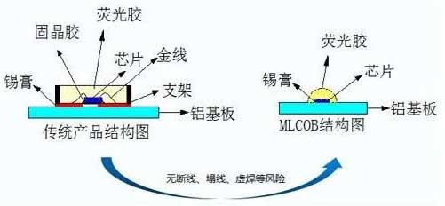
It can be said that if LED screen companies want to achieve mass production of P0.X micro pitch, formal technology obviously cannot meet their requirements, and small-sized light beads are already close to the ceiling. Therefore, some LED manufacturers have begun to develop flip chip packaging technology. As flip chip technology directly bonds the light-emitting chip with the solder pads of the PCB board, coupled with the wire free packaging process, the soldering area increases from point to surface, greatly increasing the soldering area and reducing solder joints, thus greatly improving the stability of high-definition LED displays.
The advantage of inverted COB lies in its ability to achieve mass production with a P0-X micro pitch, higher reliability, no solder wire space in the packaging layer, no glare from the surface light source, reduced thermal resistance, thinner and lighter packaging layer, better stability, higher protection level, as well as features such as collision prevention, shock resistance, dust prevention, anti-static, water and smoke prevention. Because COB packaging technology itself is embedded inside the PCB board, there will be no obvious unevenness when touched, and it can withstand higher intensity and frequency of touch operations without worrying about damaging the light beads during the touch process.
Inverted COB is also known as true chip packaging because it does not require wiring and its physical space size is only limited by the size of the light-emitting chip, allowing for packaging with smaller spacing. To a large extent, it has laid a solid foundation for touch screens. With the increasing maturity of flip chip technology, some manufacturers have begun to develop flip chip SMD technology. However, due to high costs, many LED display manufacturers still use COB flip chip technology.

Comparison of Traditional SMD Packaging and COB Inverted Technology Packaging Structure Schematics
However, this does not necessarily mean that inverted COB technology has no drawbacks. Regardless of the technology, there will be drawbacks, and inverted COB is no exception. Due to the difference between inverted COB packaging technology and traditional SMD packaging technology, higher equipment requirements are required. LED manufacturers need to address the operational risks brought by replacement and upgrading, but it will also bring great development opportunities for manufacturers. After all, COB inversion technology is an improvement on the basis of formal COB, but it also inherits the shortcomings of formal COB, such as the inability to repair a single lamp and uneven ink color. Although inverted COB has obvious drawbacks, compared to other packaging technologies, inverted COB can achieve touch technology. With the continuous reduction of dot spacing, inverted COB technology will become increasingly mature and commercialized.
In summary, with the upgrading of user consumption, the support of 5G+8k technology, and the increasing demand for ultra high definition display products in the market, LED displays are developing towards small spacing and then micro spacing. However, with the continuous reduction of spacing, traditional SMD, four in one Mini LED, and COB technologies will encounter various drawbacks. Inverted LED electronic large screen technology makes it possible for P0.X to go from scratch to mass production, and it is also beneficial for LED display manufacturers to develop touch screens.